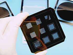
√Photomask is a high-precision plate with micro circuit, which is made of quartz plate or glass plate with a layer of chromium on the surface. The residual chromium after etching is the designed micro electrogram. This method of plate making is called light transmission in mask industry.
√Photomask is used in chip manufacturing, mainly IC chip, flat panel display, thin film magnetic head and PC board.
√The function of photomask is similar to that of film to photo. Lithography develops on the chip through photomask. If the pattern is developed multiple times on both sides of the chip through a mask, this method is known as exposure, and the mask at this time can also be called a light mask.
√The typical processes of chromium deposition on glass, photoresist deposition, electron beam lithography, and the like are the preparation of metal plates.
√TFT-LCD, CF, CSTN-LCD, STN-LCD, TN-LCD, El, OLED, PDP, VFD and other flat panel display industries;
√HDI, FPC and other printed circuit board industry;
√IC bumping, IC substrate, wire rack and other IC related industries;
√Fine electronic components industry such as Mens, sensor and enoder.


