Target
Semiconductor and related supporting manufacturers, optical coating processing enterprises


Solution

Semiconductor and related supporting manufacturers, optical coating processing enterprises
Provide PVD coating equipment and technology for enterprises
According to the characteristics of semiconductor industry products and growing customer demand, we have developed a variety of equipment technology and coating process

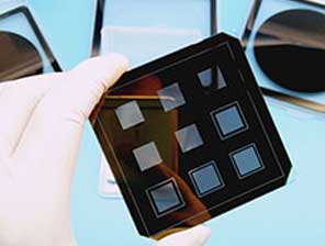
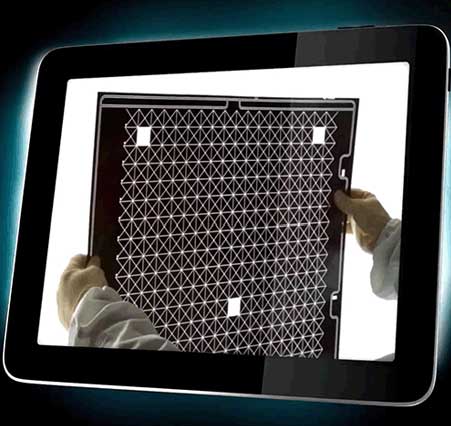
The photomask is a high-precision plate with micro circuit, which is made of quartz plate or glass plate with a layer of chromium on the surface. The residual chromium after etching is the designed micro electrogram. This plate making method is called light transmission in the mask industry.
Photomask is used in chip manufacturing, mainly IC (integrated circuit) chip, as well as flat panel display, thin film head and PC board.
The function of photomask is similar to that of negative film to photo. Photolithography develops on chip by photomask. If the pattern is developed multiple times on both sides of the chip through a mask, this method is known as exposure, and the mask at this time can also be called a mask.
The chromium film is deposited on the flat glass plate and prepared by the method similar to photoplate making. The process of the preparation is a typical lithography process, including metal PVD deposition, coating, electron beam lithography, development, chromium layer corrosion and degumming.
Chrome plate is mainly used for:
TFT-LCD, CF, CSTN-LCD, STN-LCD, TN-LCD, El, OLED, PDP, VFD and other flat panel display industries;
HDI, FPC and other printed circuit board industries;
IC bumping, IC substrate, wire rack and other IC related industries;
Mens, sensor, enoder and other fine electronic components industry.
